Scientists Have Created the World’s Most High-Performance Cell Phone
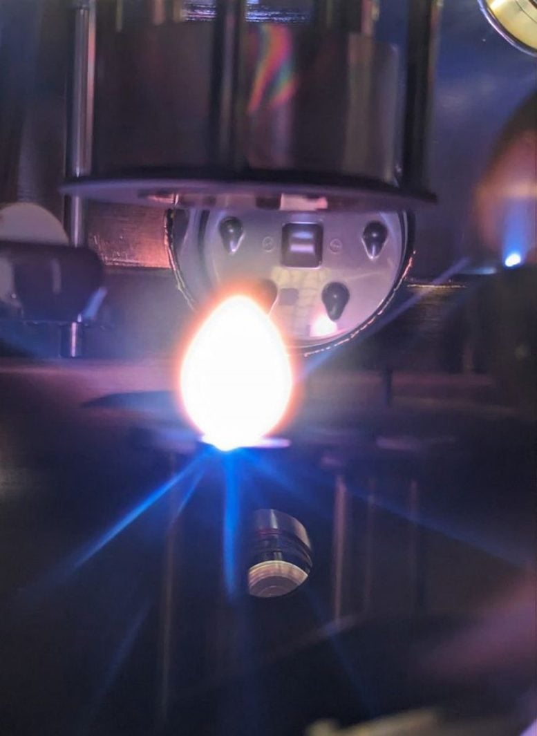
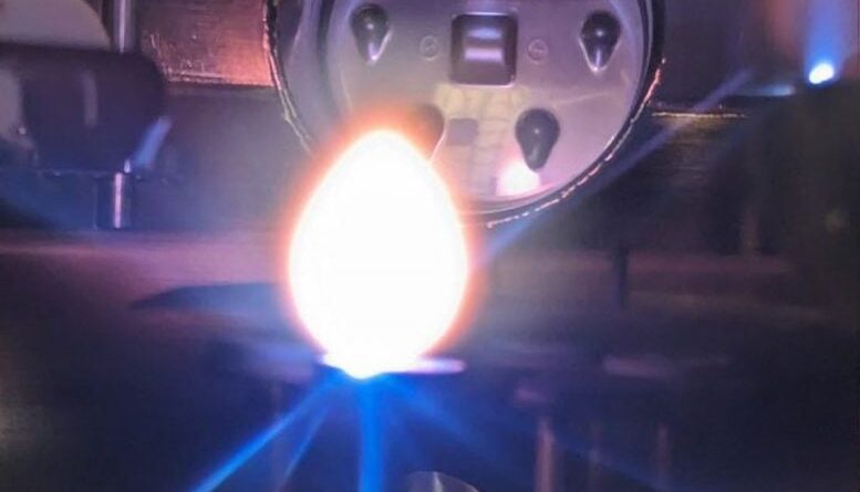
Pulsed laser deposition, where a laser light extinguishes a material deposited as a film on a substrate, was used to fabricate HTS wires. Credit: University at Buffalo
New research reveals that large-scale, low-cost implementation of high-temperature wire is still possible.
The future of our energy systems can be shaped by high-temperature heat transfer (HTS) cables. These advanced materials, capable of transmitting electricity without a higher temperature resistance than conventional superconductors, have the potential to revolutionize the power grid and make nuclear fusion a reality. the real one.
However these large scale applications will not be possible until HTS cables can be manufactured in the same price metric as the plain copper wire sold at your local hardware store.
New University at Buffalo-led research brings us closer to that goal. In a study published in Nature Communicationresearchers report that they have created the world’s most efficient HTS mobile unit while making the price performance metric excellent.
Based on rare-earth barium copper oxide (REBCO), their cables have achieved the highest current strength and pinning power – the amount of installed voltage and the ability to lower magnetic waves, respectively – recorded so far for gravity and temperature from. 5 kelvin to 77 kelvin.
This temperature is still very cold – minus 451 to 321 degrees Fahrenheit – but it is higher a full note that traditional superconductors work on.
“These results will help the industry to improve their positioning and strategies to significantly improve the price performance metric of commercial covered conductors,” said study co-author Amit Goyal. PhD, SUNY Distinguished Professor and SUNY Empire Innovation Professor. Department of Chemical and Biological Engineering, within the UB School of Engineering and Applied Sciences. “Making the cost-performance metric appropriate is necessary to fully realize many of the large-scale, envisioned applications of superconductors.”
HTS cables have many applications
HTS cable applications include power generation, such as dual power generation from offshore wind generators; grid-scale superconducting magnetic energy-storage systems; power transmission, such as lossless power transmission in high current DC and AC lines; and energy efficiency in the form of high efficiency transformers, motors and line fault limiters.
One application of HTS cables, commercial nuclear fusion, has the potential to produce unlimited clean energy. In the past few years, about 20 private companies have been established worldwide to create commercial nuclear reactors, and billions of dollars have been invested in developing HTS cables for use. just this one.
Other applications of HTS cables include next-generation MRI for medicine, next-generation nuclear magnetic resonance (NMR) for drug discovery, and advanced magnets for many physics applications. There are also many security applications, such as the development of all-electric ships and all-electric aircraft.
Currently, many companies around the world are building high-efficiency, kilometer-long HTS cables using one or more of the latest technologies developed by Goyal and his team. .
These include rolling assisted biaxially textured substrates (RABiTS) technology, ion-beam assisted deposition (IBAD) MgO technology enabled by LMOe, and nanocolumnar defects in. nanoscale simultaneous segmentation and problem-driven clustering technology.
World record for current strength and pinning strength
In the current work reported in Nature Communications, Goyal’s team reports on high-performance, superconducting wires based on REBCO.
At 4.2 kelvin, HTS cables carried 190 million amps per square centimeter without external magnetic field, also known as “self-field”, and 90 million amps per square centimeter which have a magnetic field of 7 tesla.
At a temperature of 20 kelvin – the expected application temperature for commercial nuclear fusion – the cables could still carry 150 million amps per square centimeter independently and more than 60 million square centimeters in 7 tesla.
Regarding the critical current, this corresponds to a section of wire 4-millimeter-wide at 4.2 kelvin with a supercurrent of 1,500 amps at self-field and 700 amps at 7 tesla. At 20 kelvin, that’s 1,200 amps in the field and 500 amps at 7 tesla.
It is important to note that the film of the HTS group, even if it is only 0.2 microns thick, can conduct a current that is comparable to that of large commercial cables with HTS film so that about 10 times.
As for the pinning force, the wires showed a strong ability to hold magnetic waves in place or in place, with a force of about 6.4 teranewtons per cubic meter at 4.2 kelvin and about 4.2 teranewtons per cubic meter at 20 kelvins, both under 7-tesla gravity. forget it.
These are the highest values of current density and pinning power recorded so far for all magnetic fields and operating temperatures from 5 kelvin to 77 kelvin.
“These results show that significant performance improvements are still possible, and thus the associated cost reductions that can be achieved with improved commercial HTS lines,” Goyal says.
How high performance wire is made
Part of the HTS wire is made of substrates using (IBAD) MgO technology and using nanocolumnar defects at the same time as phase separation and strain adjustment technology. Self-assembly technology allows for the inclusion of insulating or passive nanocolumns at nan0scale spacings in the superconductor. These nanodefects can spin up superconducting vortices, allowing for high supercurrents.
“The high current problem is caused by a combination of effects from rare earth doping, oxygen doping defects, and barium zirconate nanocolumns and their morphologies,” says Goyal.
“The HTS film was created using an advanced pulsed laser deposition system with careful control of the deposition parameters,” added Rohit Kumar, a fellow in the UB Laboratory of Heteroepitaxial Growth of Functional Materials. and Devices, which Goyal heads.
In pulsed laser deposition, a laser beam penetrates the target material and burns the deposited material as a film on a properly deposited substrate.
“We also performed atomic resolution microscopy using the most advanced microscopes at the Canadian Center for Electron Microscopy at McMaster University to identify nanocolumnar defects at the atomic level and performed high-resolution material measurements with at the Università di Salerno in Italy,” Goyal says. .
Reference: “Significantly improved current capacity and pinning capacity in nanostructured, (RE)BCO-based, coated conductor” by A. Goyal, R. Kumar, H. Yuan, N. Hamada, A. Galluzzi and M. Polichetti, 7 August 2024, Nature Communication.
DOI: 10.1038/s41467-024-50838-4
The Office of Army Research (ONR) supported this basic research on the development of high-resolution HTS cables. Goyal is the principal investigator on the project.
#Scientists #Created #Worlds #HighPerformance #Cell #Phone